| dc.contributor.author | Summanwar, Anand | |
| dc.contributor.author | Lietaer, Nicolas | |
| dc.date.accessioned | 2017-02-13T10:01:41Z | |
| dc.date.available | 2017-02-13T10:01:41Z | |
| dc.date.created | 2015-09-24T20:52:21Z | |
| dc.date.issued | 2011 | |
| dc.identifier.citation | Micromechanics and Micro systems Europe Workshop (MME) | nb_NO |
| dc.identifier.uri | http://hdl.handle.net/11250/2430418 | |
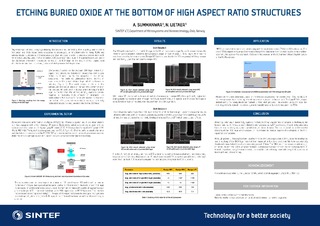
| dc.description.abstract | Plasma based dry etching is a key process widely used in micro-fabrication today. In this article, we look at the challenges involved in the anisotropic etching of buried SiO2 layers at the bottom of high aspect ratio structures on SOI wa-fers. We present our etch results that show the limitations of using a process with radio frequency (RF) substrate bias. This is followed by results obtained with a newly developed dielectric etch process based on a pulsed low frequency (LF) bias which makes it possible to etch through even rela-tively thick buried oxide layers. Finally we present an application in which this newly developed process was used. | |
| dc.description.abstract | Etching buried oxide at the bottom of high aspect ratio structures | |
| dc.language.iso | eng | nb_NO |
| dc.title | Etching buried oxide at the bottom of high aspect ratio structures | nb_NO |
| dc.type | Lecture | nb_NO |
| dc.identifier.cristin | 1272875 | |
| cristin.unitcode | 7401,90,31,0 | |
| cristin.unitname | Mikrosystemer og nanoteknologi | |
| cristin.ispublished | true | |
| cristin.fulltext | postprint | |
