3D Integration Technologies for Wireless Sensor Systems (e-CUBES)
Lecture
Permanent lenke
http://hdl.handle.net/11250/2431425Utgivelsesdato
2008Metadata
Vis full innførselSamlinger
- Publikasjoner fra CRIStin - SINTEF AS [5801]
- SINTEF Digital [2501]
Originalversjon
IMAPS Int. Conf. Device PackagingSammendrag
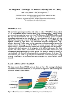
The innovative approach presented here will realize so-called e-CUBES® (electronic cubes) [1], i.e. investigate and develop ultra small sensor cubes with dimensions of a few mm3 which are wirelessly communicating among each other. The fabrication of e-CUBES with their need for high-level miniaturization (see Fig. 1) can only be realized by system integration technologies, which use the third dimension: 3D System Integration. In general not only one 3D integration technology is suitable for the fabrication of the large variety of 3D integrated systems. Moreover, a single product may need several different technologies for a cost-effective fabrication. Wireless sensor systems represent an excellent example for the need of a suitable mixture. Consisting of MEMS, ASICs, memories, antennas, and power supply modules they can only be fabricated in a cost-effective way by application of 3D technologies, which are particularly optimized for the integration of the different sub-modules. The main objective is to achieve extreme miniaturization of wireless sensor nodes. In consequence, all wiring should be realized through the stacked devices. Wire bonds are replaced by through-Si vias combined with electrical and mechanical interconnections between the devices. The removal of long wire bonds is especially beneficial for sensors based on a capacitive sensing principle (rather than i.e. a piezo-resistive sensing principle), since parasitic effects will be reduced. 3D Integration Technologies for Wireless Sensor Systems (e-CUBES)
