| dc.contributor.author | Johnsen, Lars | |
| dc.contributor.author | Gastinger, Kay | |
| dc.date.accessioned | 2017-02-13T13:30:11Z | |
| dc.date.available | 2017-02-13T13:30:11Z | |
| dc.date.created | 2015-09-24T20:35:49Z | |
| dc.date.issued | 2010 | |
| dc.identifier.citation | 25th European Photovoltaic Solar Energy Conference and Exhibition | nb_NO |
| dc.identifier.uri | http://hdl.handle.net/11250/2430608 | |
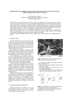
| dc.description.abstract | A setup for high resolution video recording of the chipping process during slurry based sawing of silicon is introduced. The setup allows in situ imaging of the chipping process in silicon (Si) by operating in the near infrared region where Si is transparent. Extended resolution is achieved through the use of a silicon lens as sample for the sawing. By sawing in the lens perfect immersion optics are implemented resulting in an imaging system with very high numerical aperture. The sample is illuminated by a halogen lamp through a beam splitter cube. An InGaAs camera with VGA resolution is used for video capturing. The paper presents a work in progress. Results from experiments with an x,y,z-controlled single indenter as well as indents from silicon carbide (SiC) particles trapped between the saw wire and the Si surface are presented. Image sequences of the dynamic development of the indent process and the consecutive chipping are presented. | |
| dc.description.abstract | MICROSCOPIC NEAR INFRARED (NIR) IMAGING FOR INVESTIGATION OF THE SAW-CHANNEL SURFACE DURING WIRE-SAWING OF SILICON | |
| dc.language.iso | eng | nb_NO |
| dc.title | MICROSCOPIC NEAR INFRARED (NIR) IMAGING FOR INVESTIGATION OF THE SAW-CHANNEL SURFACE DURING WIRE-SAWING OF SILICON | nb_NO |
| dc.type | Lecture | nb_NO |
| dc.identifier.cristin | 1272525 | |
| cristin.unitcode | 7401,90,41,0 | |
| cristin.unitname | Optiske målesystemer og dataanalyse | |
| cristin.ispublished | true | |
| cristin.fulltext | postprint | |