| dc.contributor.author | Lietaer, Nicolas | |
| dc.contributor.author | Summanwar, Anand | |
| dc.contributor.author | Dalsjø, Per G. | |
| dc.contributor.author | Bakke, Thor | |
| dc.contributor.author | Tofteberg, Hannah Rosquist | |
| dc.date.accessioned | 2017-02-08T10:48:15Z | |
| dc.date.available | 2017-02-08T10:48:15Z | |
| dc.date.created | 2011-01-26T13:47:33Z | |
| dc.date.issued | 2010 | |
| dc.identifier.uri | http://hdl.handle.net/11250/2429936 | |
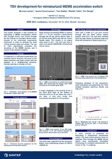
| dc.description.abstract | Fragile micromachined MEMS structures are usually protected by bonding a capping wafer to the device wafer itself. As opposed to using lateral interconnects at the interface between the cap wafer and the device wafer, the use of vertical through silicon vias (TSVs) significantly simplifies the mounting of the components and it also results in the smallest footprint. This paper presents the concept chosen for fabricating a miniaturized MEMS acceleration switch with TSVs through the SOI (silicon on insulator) device wafer, as well as the experimental results of the TSV process development that was done for this particular application. Especially challenging was the development of an etching process that can etch the thick buried oxide of the SOI wafer through high aspect ratio trenches. | |
| dc.language.iso | eng | nb_NO |
| dc.title | TSV development for miniaturized MEMS acceleration switch | nb_NO |
| dc.type | Lecture | nb_NO |
| dc.identifier.cristin | 531722 | |
| cristin.unitcode | 7401,90,31,0 | |
| cristin.unitname | Mikrosystemer og nanoteknologi | |
| cristin.ispublished | true | |
| cristin.fulltext | original | |
